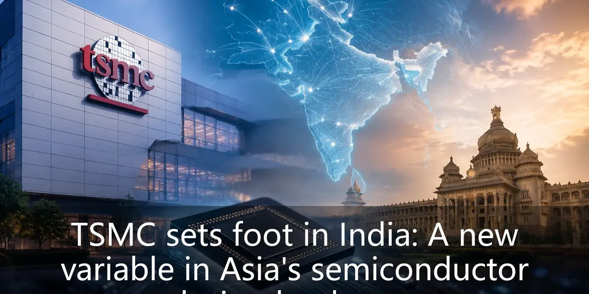
TSMC Announces AI Chip Design R&D Center in India
On July 28, 2026, TSMC officially announced that it will establish its first R&D center in South Asia in Bangalore, India, focusing on AI chip design. This move marks a new chapter in TSMC's global strategy of extending from manufacturing to design services, and is also the latest result of India's semiconductor industry policy attracting international giants.
India Expansion: Strategic Considerations and Resource Integration
TSMC's India R&D center will mainly focus on AI accelerators, edge computing chips, and high-throughput computing architecture design under advanced process nodes. Bangalore, as India's "Silicon Valley," has a global talent pool of chip design engineers, including senior engineers from Intel, AMD, NVIDIA, etc. TSMC CEO C.C. Wei stated in the announcement: "India has world-class IC design talent, which combined with TSMC's manufacturing process, will accelerate AI chip innovation."
The R&D center will have an initial investment of about $500 million, aiming to recruit 2,000 design engineers by the end of 2027, and will collaborate with local universities such as the Indian Institutes of Technology (IIT). India's Ministry of Electronics and Information Technology (MeitY) previously launched the "India Semiconductor Mission," offering capital subsidies of up to 50%, which was a key factor attracting TSMC.
Dual Advantages of Talent and Cost
The average salary of chip design engineers in India is only 60% of that in Taiwan, and about 30,000 related graduates are added annually. By setting up a design center in India, TSMC can reduce R&D costs and ease the shortage of design talent in Taiwan. Industry analysts point out that TSMC previously relied mainly on design teams in Hsinchu, Taiwan and Yokohama, Japan; the addition of the Indian team will enable global 24/7 design.
Impact on Asian Semiconductor Industry Landscape
TSMC's India move is seen by the industry as a microcosm of the Asian semiconductor industry's shift from "manufacturing concentration" to "design dispersion." For a long time, Asian semiconductor design centers have been mainly concentrated in Taiwan, South Korea, Mainland China, and Singapore. Although India leads in software services, high-end chip design has remained at the low end of the value chain. TSMC's entry will drive the rise of a batch of local design startups.
Complementing India's "Chip Manufacturing Dream"
Notably, TSMC did not set up a wafer fab in India but chose a design center. This complements the Indian government's goal of attracting manufacturing. India currently has a 28nm wafer fab jointly built by Tata Group and Foxconn, but advanced process nodes (below 7nm) are still unavailable. TSMC's design center will provide India with full services from design to tape-out, helping Indian chip companies use TSMC's advanced process without outsourcing design teams overseas.
Competitors' Reactions
TSMC's move has also prompted South Korea's Samsung Electronics and the US company GlobalFoundries to follow suit. Samsung recently announced expansion of its packaging and testing plant in Chennai, India, and plans to set up an AI chip design team. GlobalFoundries has partnered with Indian startup Mindgrove to develop autonomous driving chips. A battle for India's chip design talent has begun.
Challenges and Uncertainties
Despite an optimistic outlook, TSMC still faces many challenges in India. First, India's infrastructure is relatively lagging; Bangalore frequently suffers from power outages and water supply issues, which may affect the stability of the design center. Second, India's data security regulations are strict; TSMC needs to ensure localized protection of customer IP (intellectual property). Additionally, geopolitical risks cannot be ignored: border tensions between India and China/Pakistan, and India's reliance on US technology amid the US-China tech decoupling, may bring uncertainties to operations.
Talent Attrition Risk
India's chip design talent has high mobility; TSMC needs to offer competitive salaries and career development paths to prevent engineers from being poached by local startups or Silicon Valley giants. An internal TSMC source revealed that the company will adopt a "mentorship system" and overseas rotation programs to enhance employee loyalty.
Future Outlook: A New Node in Asian Semiconductor Design
The establishment of TSMC's India R&D center is not only an enterprise-level expansion but also likely to elevate India to the fourth-largest semiconductor design hub in Asia (after Taiwan, South Korea, and Mainland China). According to IC Insights, by 2028, the market size of India's self-designed chips will exceed $30 billion, with AI chips accounting for over 40%.
For Asian semiconductor capital, this event signals a shift in investment logic: from simply pursuing manufacturing capacity to building design capabilities and talent ecosystems. Analysts at Saiph Semiconductor News believe that over the next three years, more than 50 global semiconductor companies will set up design centers in India, making India a key battleground for AI chip design.
Response from China's Semiconductor Industry
TSMC's expansion in India also serves as a wake-up call for China's semiconductor industry. China currently has the largest number of IC design companies globally, but still faces limitations in advanced process design capabilities. India, with its English advantage and Western value alignment, can more easily obtain TSMC's advanced design support. China should accelerate the development of local EDA tools and IP cores, and deepen talent cooperation with Southeast Asia and the Middle East to maintain competitiveness.
Conclusion
TSMC's move into India is a milestone event for the Asian semiconductor industry's shift from "manufacturing first" to "design-led." In the AI wave sweeping the globe in 2026, those who master design talent will take the initiative in the second half of the chip industry. Saiph Semiconductor News will continue to follow this development and bring readers in-depth interpretation.